

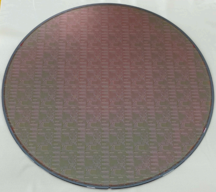
8inch Thin film LN/LT on Silicon Photonics
Main Application: High performance filters for mobile communications. (POI/LTOI)
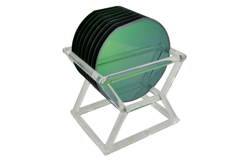
Main Application : TFLN electro-optic modulator, Nonlinear optics, Quantum devices, etc. (LNOI)
Composite structure of monocrystalline silicon thin film and silicon-based lithium niobate (LNOI)
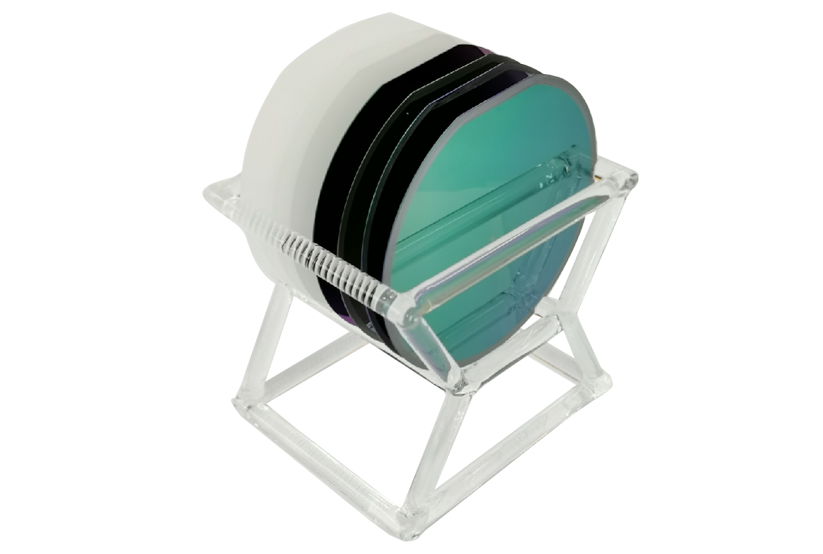
TFLN on Quartz, Sapphire, SiC
Er-doped LNOI, Erbium-doped LNOI
MgO-doped LNOI, Magnesium oxide doped LNOI
• 50-400keV
• 2, 3, 4, 6, 8 inch
• TTV<1 um
• 4, 6, 8 inch
• Si, LN, LT, etc.
• RMS<0.5nm
• 4, 6, 8 inch
• Si, SiO2, LT, LN, etc.
• SiC, LN, LT, etc.
Inno Semiconductor Technology, established in 2021, is located in Jiading District, Shanghai, China. Inno Semiconductor Technology is committed to promoting the commercialization of heterogeneous integrated material substrate. At present, our main products include high-performance micro acoustic chip materials and high-speed optical communication chip materials.